
An Interest In:
Web News this Week
- April 26, 2024
- April 25, 2024
- April 24, 2024
- April 23, 2024
- April 22, 2024
- April 21, 2024
- April 20, 2024
Some of Our Sources
- Pearsonified
- Spoon Graphics
- Creative Curio
- Noupe
- Web Design Ledger
- CSS Globe
- Line 25
- Stylized Web
- The Verge
- TechPowerUp
Help Webnuz
Referal links:
Nanofabrication (Semiconductor) Wafer Thickness Prediction Data
Open Data Sets in Micro-nano fabrication Part II
Introduction
The manufacturing industry is always thriving on solving interesting problems with Data and Analytics solutions. Measuring the critical dimension of materials under a product line is one such problem. The problem becomes interesting when the measurements are accurate and minute in nm (nanometer) scales. The semiconductor industry has such a problem measuring thin film thickness during the manufacturing cycle. It is a domain-centric and Intellectual Property(IP) driven area due to the competitive nature of the industry. There are proven solutions available, and known industry leaders are there in the space like KLA and Filmetrics. After many decades it is the first time a large open data-set to solve the problem by the Data Science Community. There was no open data-set available in the industry, which was not an innovation blocker. There are enough research materials produced by academia and industry. It was opened up. The data will be beneficial in training Process Engineers and Data Analysts in Semiconductor industry problem-solving.
Nanofabrication and Thickness
Semiconductors are the backbones of modern digital infrastructure. The very industry is powered by fundamental science such as research on material sciences, physics, chemistry, and mechanics. A fair understanding of this fundamental science is required in solving Nanofabrication/Semiconductor AI/ML problems (the industry knowledge). The due natural course of evolution Information Technology (IT), Data and Analytics, and Artificial Intelligence started complementing the field and vice versa.
The process of martial modification is similar to the 'edit distance' concept in Text processing. Materials are selectively added, removed, or modified to create minute structures under controlled environments. Measuring various materials' thickness is critical to improving the manufacturing yield during each stage of this sequence. The thickness we discuss here is <1 nm to 100 mm (thickness of human hair) thick. There are many processes in the Nanofabrication industry, such as Physical Vapor Deposition (PVD or Sputtering)[4], Etching, spin coating, etc. To achieve the target functionality of a semiconductor chip, maintaining accurate measurements (in nm)are a strict requirement. The industry refers to this under the blanket problem 'Yield Improvement .' Once again, AI or ML alone is not the silver bullet to solve the problem; a harmonic collaboration of Material Scientists, Process Engineers, and Data Analytics professionals is required.
One of the key concepts from Physics to refresh to understand the data is reflectance. Reflectance is the fraction of incident light reflected from a surface, and it is an intrinsic property of thin films[5].
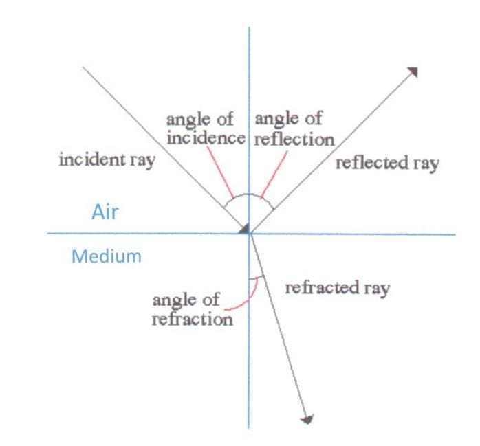
Image 1- Reflection and refraction of light at a boundary between two media[5].
The concept is very critical in understanding the thickness data discussed here. Exemplary details of the reflectance are discussed in reference [5] and the metrology guide by Filmetrics[6], which is worth reading for domain understanding. Optical spectrum analysis is one widely used method to measure thin film thickness. Domain knowledge, computing resources, and subject matter expertise are required to perform the operations. If a subject matter expert in the loop process is adopted, the measurement process is relatively time-consuming.
Dacon Thin Film Thickness Data
The Dacon [1], a Korean data science competition platform like Kaggle, launched a 'Semiconductor think film thickness analysis contest' [2]. Considering all the IP-centric nature, they abstracted the data preserving the nature of the problem. The data is available on the Dacon competition page, subject to terms and conditions[2].
Format
The data was part of a competition, and the organizers provided data in two comma-separated value (CSV) files. The first file was training data with four target thickness measurements and test data without the target. The training file consists of 810k observations with 230 attributes, out of which four attributes are the thickness measurement. The test data-set which is meant for final submission is only 1k records.
Data Attributes
The first four attributes measure the thickness of the four layers layer_1 through 4. The unit of measurement is nm in scale. The materials under reference for this measurement are Si3N4 (Silicon Nitrate), SiO2 (Silicon Dioxide), Si3N4 (Silicon Nitride), and SiO2. The rest of the attributes are masked values to protect IP. These values are expressed as wavenumber (reciprocal of wavelength). The column names are 0~255, and it is between 285 to 800 nm. A plot of the random record is provided below. This plot represents reflectance in y, and x represents the values 0~255 in the data.
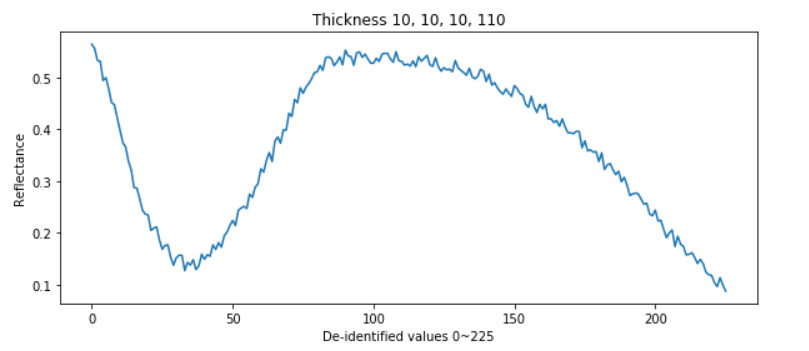
Image 2- Thickness data sample.
The Data Context
It is always better to understand the context of data, such as how it is generated measured is always essential in AI/ML experiments. In this process data context, we are trying to predict the measurements of four layers. In processes condition, the bottom layer is always Si (Silicon) and Air in the top layer. Let us find the theoretical reflectance from the four layers to understand this better. I will be using the tool available from Filmetrics [3] to get the theoretical reference range.
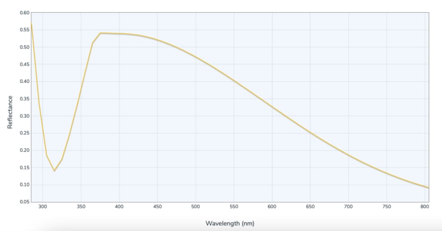
Image 3- Theoretical reflectance range for the Dacon data record data shown above
Now we can spot the similarity between the data. In my original plot, I reversed the 0~255 after referring to the Filmetrics reference plot. Since this data is the refraction of light, it is essential to know the angle of incidence. The angle of incidence is 0 degrees in the data.
Observation
One of the interesting observations about the data after checking the Filmetrics plot was a reversal. It may not be necessary to reverse the data for the ML experiment. The Dacon data was changed as part of the de-identification process. To confirm the same, I plotted more than 25 randomly drawn samples from the training data, compared with the Filmetrics plot.
Missing Information
As part of IP protection, the team provided necessary details only. A detailed study and additional modeling information, such as the process information and machinery used to collect the data, etc., might have added more context to the data. A Machine Learning professional will access such minute context details in a real-world situation.
Predicting Thin Film Thickness
After we understand the data, it is time for building some models. In this data scenario, there is some room for feature engineering. I am leaving this for the larger reader community as I intend to introduce the data and domain. I created a reference model as a starter and provided references to the GitHub repository for other implementations.
We use the type of regression strategy called Multi-Output Regression [7]. The problem is unique as it is a regression case but predicts multiple targets. Both classical and Deep Learning methodologies are very effective in solving multi-output regression. In my reference implementation, I used the scikit-learn(sklearn) MultiOutPutRegression API along with the XGBoost library.
The notebook is available at - https://github.com/jaganadhg/waferthickness
If you are interested in solutions by some of the solutions by competitions participants, please refer to the following GitHub repositories.
https://github.com/YoonSungLee/DACON-semiconductor-competition
https://github.com/pjhsk113/DACON-Semiconductor-Thinfilm-Analysis
https://github.com/popo97kr/DACON_semiconductor
I am looking forward to exciting findings and research papers from the data.
Acknowledgment
I am grateful to the AWS Community Builder Program for providing SageMaker and AWS credits. I used AWS SageMaker for Exploratory Data Analysis and Machine Learning experiments. I used Google Translate (from Korean to English) to understand the data and studied many community posts in the Dacon competition forum. Some of the graphing insights are derived from the clarifications provided by the Dacon team and a user' dodo'. I acknowledge the knowledge sharing by the Dacon user community, which helped me create the content.
Competing Interests
The authors declare that no proprietary information related to the authors, affiliated company, or its approach, methodologies, and IPR is discussed in these notes. The authors declare that they have no competing interests.
How to Cite
[*] Jaganadh Gopinadhan, Nanofabrication (Semiconductor) Wafer Thickness Prediction Data, Open Data Sets in Micro-nano fabrication Part II.
References
[2] https://dacon.io/competitions/official/235554/overview/description/
[3] https://www.filmetrics.com/reflectance-calculator
[4] https://www.sciencedirect.com/topics/materials-science/sputter-deposition
[5] Reflectance in Thin Films - https://materion.com/-/media/files/advanced-materials-group/me/technicalpapers/reflectance-in-thin-films_all.pdf
[6] Thin Film Measurements - https://files.filmetrics.com/pdf/Filmetrics%20Tutorial%20-%20Thickness%20Metrology%20Guide%20v3N.pdf
[7] Machine learning Refined - https://www.cambridge.org/highereducation/books/machine-learning-refined/0A64B2370C2F7CE3ACF535835E9D7955#overview
Original Link: https://dev.to/aws-builders/nanofabrication-semiconductor-wafer-thickness-prediction-data-am
Dev To
More About this Source Visit Dev To