
An Interest In:
Web News this Week
- April 20, 2024
- April 19, 2024
- April 18, 2024
- April 17, 2024
- April 16, 2024
- April 15, 2024
- April 14, 2024
Some of Our Sources
- Web Designer Wall
- Just Creative
- Pearsonified
- Smashing Apps
- Crazy Leaf Design
- Wal You
- Design Modo
- Android Dissected
- The Verge
- TechPowerUp
Help Webnuz
Referal links:
June 30, 2022 06:07 am GMT
"Samsung has grown rapidly as we continue to demonstrate leadership in applying next-generation technologies to manufacturing, such as foundry industry's first High-K Metal Gate, FinFET, as well as EUV. We seek to continue this leadership with the world's first 3 nm process with the MBCFET," said Dr. Siyoung Choi, President and Head of Foundry Business at Samsung Electronics. "We will continue active innovation in competitive technology development and build processes that help expedite achieving maturity of technology."


Original Link: https://www.techpowerup.com/296345/samsung-begins-chip-production-using-3nm-process-technology-with-gaa-architecture
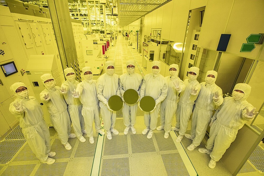
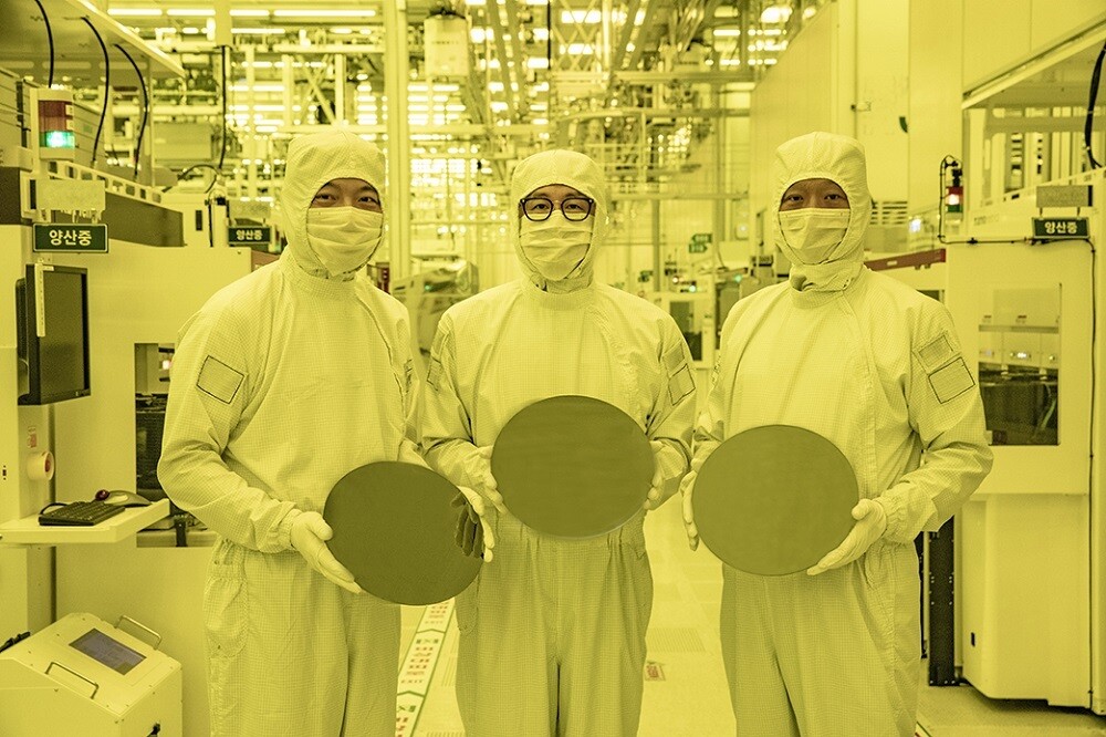
(PR) Samsung Begins Chip Production Using 3nm Process Technology With GAA Architecture
Samsung Electronics, the world leader in semiconductor technology, today announced that it has started initial production of its 3-nanometer (nm) process node applying Gate-All-Around (GAA) transistor architecture. Multi-Bridge-Channel FET (MBCFET ), Samsung's GAA technology implemented for the first time ever, defies the performance limitations of FinFET, improving power efficiency by reducing the supply voltage level, while also enhancing performance by increasing drive current capability. Samsung is starting the first application of the nanosheet transistor with semiconductor chips for high performance, low power computing application and plans to expand to mobile processors."Samsung has grown rapidly as we continue to demonstrate leadership in applying next-generation technologies to manufacturing, such as foundry industry's first High-K Metal Gate, FinFET, as well as EUV. We seek to continue this leadership with the world's first 3 nm process with the MBCFET," said Dr. Siyoung Choi, President and Head of Foundry Business at Samsung Electronics. "We will continue active innovation in competitive technology development and build processes that help expedite achieving maturity of technology."


Original Link: https://www.techpowerup.com/296345/samsung-begins-chip-production-using-3nm-process-technology-with-gaa-architecture
Share this article:
Tweet

View Full Article