
An Interest In:
Web News this Week
- April 19, 2024
- April 18, 2024
- April 17, 2024
- April 16, 2024
- April 15, 2024
- April 14, 2024
- April 13, 2024
Some of Our Sources
- Simplebits
- Joshua Blankenship
- Pearsonified
- Creative Curio
- Web Designer Depot
- Fudge Graphics
- CSS Globe
- Specky Boy
- Daily Now
- The Verge
Help Webnuz
Referal links:
January 29, 2022 04:37 pm GMT
If this is indeed the case and NVIDIA isn't deploying a MCM (Multi-Chip Module) design on Hopper, which is designed for a market with increased profit margins, it likely means that less profitable consumer-oriented products from NVIDIA won't be featuring the technology either. MCM designs also make more sense in NVIDIA's HPC products, as they would enable higher theoretical performance when scaling - exactly what that market demands. Of course, NVIDIA could be looking to develop an MCM version of the GH100 still; but if that were to happen, the company could be looking to pair two of these chips together as another HPC product (rumored GH-102). ~2,000 mm in a single GPU package, paired with increased density and architectural improvements might actually be what NVIDIA requires to achieve the 3x performance jump from the Ampere-based A100 the company is reportedly targeting.
Original Link: https://www.techpowerup.com/291440/nvidia-hopper-might-have-huge-1000-mm-die-monolithic-design
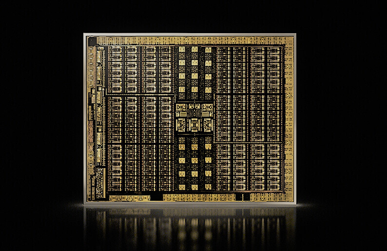
NVIDIA "Hopper" Might Have Huge 1000 mm Die, Monolithic Design
Renowned hardware leaker kopike7kimi on Twitter revealed some purported details on NVIDIA's next-generation architecture for HPC (High Performance Computing), Hopper. According to the leaker, Hopper is still sporting a classic monolithic die design despite previous rumors, and it appears that NVIDIA's performance targets have led to the creation of a monstrous, ~1000 mm die package for the GH100 chip, which usually maxes out the complexity and performance that can be achieved on a particular manufacturing process. This is despite the fact that Hopper is also rumored to be manufactured under TSMC's 5 nm technology, thus achieving higher transistor density and power efficiency compared to the 8 nm Samsung process that NVIDIA is currently contracting. At the very least, it means that the final die will be bigger than the already enormous 826 mm of NVIDIA's GA100.If this is indeed the case and NVIDIA isn't deploying a MCM (Multi-Chip Module) design on Hopper, which is designed for a market with increased profit margins, it likely means that less profitable consumer-oriented products from NVIDIA won't be featuring the technology either. MCM designs also make more sense in NVIDIA's HPC products, as they would enable higher theoretical performance when scaling - exactly what that market demands. Of course, NVIDIA could be looking to develop an MCM version of the GH100 still; but if that were to happen, the company could be looking to pair two of these chips together as another HPC product (rumored GH-102). ~2,000 mm in a single GPU package, paired with increased density and architectural improvements might actually be what NVIDIA requires to achieve the 3x performance jump from the Ampere-based A100 the company is reportedly targeting.
Original Link: https://www.techpowerup.com/291440/nvidia-hopper-might-have-huge-1000-mm-die-monolithic-design
Share this article:
Tweet

View Full Article