
An Interest In:
Web News this Week
- April 18, 2024
- April 17, 2024
- April 16, 2024
- April 15, 2024
- April 14, 2024
- April 13, 2024
- April 12, 2024
Some of Our Sources
- Mashable
- Technology Review
- Simplebits
- Just Creative
- Joshua Blankenship
- Smashing Magazine
- Creative Curio
- Fudge Graphics
- Stylized Web
- Android Dissected
Help Webnuz
Referal links:
March 23, 2021 05:00 pm GMT
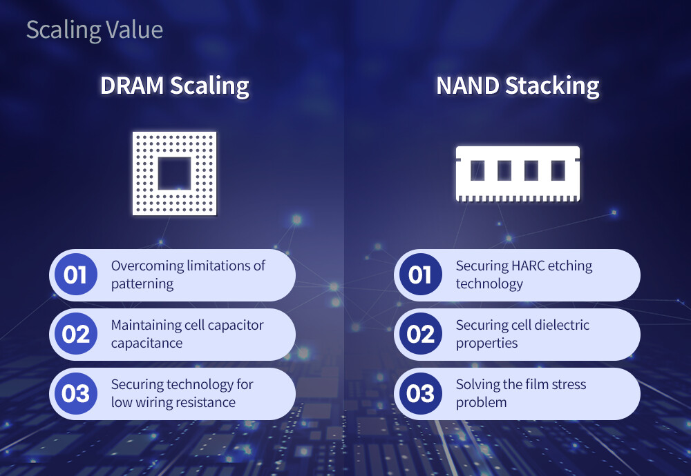
So far, the company has managed to manufacture and sample 512Gb 176-layer 3D NAND chips, so the 600-layer solutions are still far away. Nonetheless, it is a possibility that we are looking at. Before we reach that layer number, there are various problems needed to be solved so the technology can work. According to SK Hynix, "the company introduced the atomic layer deposition (ALD) technology to further improve the cell property of efficiently storing electric charges and exporting them when needed, while developing technology to maintain uniform electric charges over a certain amount through the innovation of dielectric materials. In addition to this, to solve film stress issues, the mechanical stress levels of films is controlled and the cell oxide-nitride (ON) material is being optimized. To deal with the interference phenomenon between cells and charge loss that occur when more cells are stacked at a limited height, SK Hynix developed the isolated-charge trap nitride (isolated-CTN) structure to enhance reliability."

Original Link: https://www.techpowerup.com/280069/sk-hynix-envisions-the-future-600-layer-3d-nand-and-euv-made-dram
SK Hynix Envisions the Future: 600-Layer 3D NAND and EUV-made DRAM
On March 22nd, the CEO of SK Hynix, Seok-Hee Lee, gave a keynote speech to the IEEE International Reliability Physics Symposium (IRPS) and shared with experts a part of its plan for the future of SK Hynix products. The CEO took the stage and delivered some conceptual technologies that the company is working on right now. At the center of the show, two distinct products stood out - 3D NAND and DRAM. So far, the company has believed that its 3D NAND scaling was very limited and that it can push up to 500 layers sometime in the future before the limit is reached. However, according to the latest research, SK Hynix will be able to produce 600-layer 3D NAND technology in the distant future.So far, the company has managed to manufacture and sample 512Gb 176-layer 3D NAND chips, so the 600-layer solutions are still far away. Nonetheless, it is a possibility that we are looking at. Before we reach that layer number, there are various problems needed to be solved so the technology can work. According to SK Hynix, "the company introduced the atomic layer deposition (ALD) technology to further improve the cell property of efficiently storing electric charges and exporting them when needed, while developing technology to maintain uniform electric charges over a certain amount through the innovation of dielectric materials. In addition to this, to solve film stress issues, the mechanical stress levels of films is controlled and the cell oxide-nitride (ON) material is being optimized. To deal with the interference phenomenon between cells and charge loss that occur when more cells are stacked at a limited height, SK Hynix developed the isolated-charge trap nitride (isolated-CTN) structure to enhance reliability."

Original Link: https://www.techpowerup.com/280069/sk-hynix-envisions-the-future-600-layer-3d-nand-and-euv-made-dram
Share this article:
Tweet

View Full Article