
An Interest In:
Web News this Week
- April 20, 2024
- April 19, 2024
- April 18, 2024
- April 17, 2024
- April 16, 2024
- April 15, 2024
- April 14, 2024
Some of Our Sources
- Engadget
- Techcrunch
- Simplebits
- TutsPlus - Code
- Team Treehouse
- Spoon Graphics
- Smashing Magazine
- Smashing Apps
- Web Design Ledger
- CSS Tricks
Help Webnuz
Referal links:
March 12, 2021 08:46 am GMT
Samsung has demonstrated the first SRAM chip that uses MBCFET technology today. The chip in question is a 256 Gb chip with an area of 56 mm. The achievement Samsung is proud of is that the chip uses 230 mV less power for writes, compared to the standard approach, as the MBCFET transistors allow the company to have many different power-saving techniques. The new 3 nm MBCFET process is expected to get into high-volume production sometime in 2022, however, we are yet to see demos of logic chips besides SRAM like we see today. Nonetheless, even the demonstration of SRAM is big progress, and we are eager to see what the company manages to build with the new technology.

Original Link: https://www.techpowerup.com/279625/samsung-demonstrates-256-gb-3-nm-mbcfet-chip-at-isscc-2021
Samsung Demonstrates 256 Gb 3 nm MBCFET Chip at ISSCC 2021
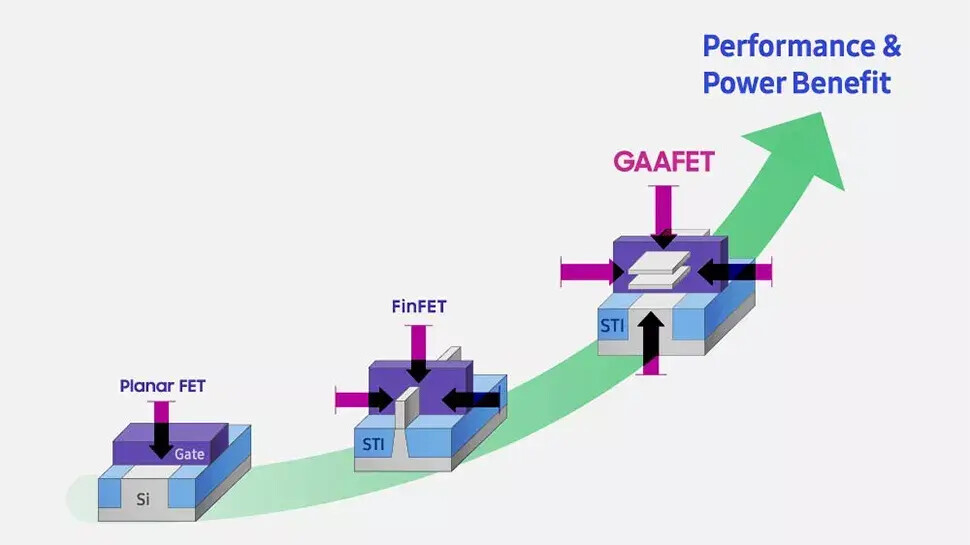
During the IEEE International Solid-State Circuits Conference (ISSCC), Samsung Foundry has presented a new step towards smaller and more efficient nodes. The new chip that was presented is a 256 Gb memory chip, based on SRAM technology. However, all of that doesn't sound interesting, until we mention the technology that is behind it. Samsung has for the first time manufactured a chip using the company's gate-all-around field-effect transistor (GAAFET) technology on the 3 nm semiconductor node. Formally, there are two types of GAAFET technology: the regular GAAFET that uses nanowires as fins of the transistor, and MBCFET (multi-bridge channel FET) that uses thicker fins that come in a form of a nanosheet.Samsung has demonstrated the first SRAM chip that uses MBCFET technology today. The chip in question is a 256 Gb chip with an area of 56 mm. The achievement Samsung is proud of is that the chip uses 230 mV less power for writes, compared to the standard approach, as the MBCFET transistors allow the company to have many different power-saving techniques. The new 3 nm MBCFET process is expected to get into high-volume production sometime in 2022, however, we are yet to see demos of logic chips besides SRAM like we see today. Nonetheless, even the demonstration of SRAM is big progress, and we are eager to see what the company manages to build with the new technology.

Original Link: https://www.techpowerup.com/279625/samsung-demonstrates-256-gb-3-nm-mbcfet-chip-at-isscc-2021
Share this article:
Tweet

View Full Article